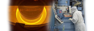
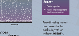
 | SUMCO
is proud to offer iGEM™, a new, internal gettering-enhanced
material to improve device yield and performance for semiconductor
manufacturers using N/N+ epitaxial wafers. Currently
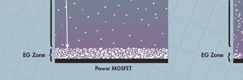
available in 150 mm diameter, iGEM™ meets the
special needs of Power MOSFET and bipolar device makers.
It has been shown to improve yield on arsenic- and antimony-doped
wafers. The properties of this silicon
substrate have been engineered to provide four critical benefits:
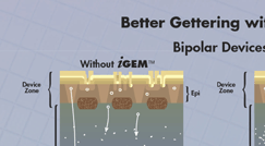
- Reduced
device junction leakage, resulting in increased device yields.
With iGEM™ wafers, you'll have less drain-to-source
(IDSS) and collector-to-emitter (ICEO) leakage.
- More
robust gettering, to stabilize device manufacturing yields
and device reliability. iGEM™ reduces variation
of critical device properties such as hFE.
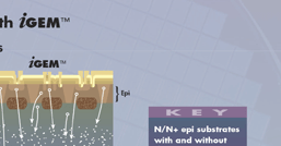
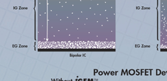
- New
levels of device performance. iGEM™ improves
gettering at various levels of low resistivity, so you can
expect improved yields at your current resistivity level
and have the ability to move to lower resistivity without
sacrificing yield or performance.
- Reduced
slip and bow, leading to better mechanical stability.
|
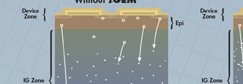
Opportunities for future savings The
engineered improvements in iGEM™complement conventional
techniques, such as thin films and backside damage that increase
gettering in low-resistivity wafers. Preliminary indications
suggest that iGEM™customers, working collaboratively
with SUMCO engineers, may be able to reduce or eliminate
other costly processes at the wafer or device manufacturing
line. This could reduce your total cost of ownership. Enjoy
immediate improvement Switching
from a conventionally gettered, low-resistivity wafer to
iGEM™is easy. It requires little or no change
in your device manufacturing processes, and may not even
require new qualification. Anticipating
the demand for this promising new product, SUMCO is fully
ramped to supply production quantities of iGEM™
wafers immediately. For information
and ordering Contact the SUMCO Account
Manager or Applications Engineer in your region. |