 | SUMCO's
MOS technology is driven by close collaboration with our
customers to identify and address their advanced products
needs. Guided by customer input and the ITRS roadmap, SUMCO's
research and development experts in Amagasaki, Imari and
Noda, Japan create proprietary technologies, which are then
transferred to SUMCO's manufacturing facilities in the U.S.
and throughout the world.
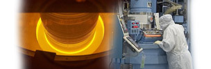
SUMCO's
state-of-the-art MOS wafers are used for a variety of applications,
including memory, microprocessors, microcontrollers, imbedded
devices and system-on-a-chip. MOS wafers are available in
125 to 300mm diameters in production volumes down to 110
and 90 nanometer (nm) geometry capability.
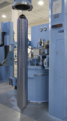
| | SUMCO's
state-of-the-art MOS products include:
- Engineered
prime polished wafers
- A
variety of epitaxial wafers
- SOI
- SIMOX and bonded wafers
- Hydrogen
and argon-annealed wafers
|
For
more information about SUMCO MOS wafer products, contact
your Account
Manager.
|